LECTURE №5
SENSORS AND SIGNAL PROCESSING.
SIGNAL CONDITIONING DEVICES
5.1. SIGNAL CONDITIONING
OPERATIONS
In previous lectures we have
studied various sensors and transducers used in a mechatronics system.
Transducers sense physical phenomenon such as rise in temperature and convert
the measurand into an electrical signal viz. voltage or current. However these
signals may not be in their appropriate forms to employ them to control a mechatronics
system. Figure 5.1.1 shows various
signal conditioning
operations which are being carried out in controlling
a mechatronics based system.
The signals given by a
transducer may be nonlinear in nature or may contain noise. Thus before sending
these signals to the mechatronics control unit it is essential to remove the
noise, nonlinearity associated with the raw output from a sensor or a transducer.
It is also needed to modify the amplitude (low/high) and form (analogue/digital)
of the output signals into respective acceptable limits and form which will be
suitable to the control system. These activities are carried out by using
signal conditioning devices and the process is termed as «signal conditioning».
Signal conditioning system
enhances the quality of signal coming from a sensor in terms of:
1. Protection (to protect the damage to the next element of
mechatronics system such microprocessors from the high current or voltage
signals);
2. Right type of signal (to
convert the output signal from a transducer into the desired form i.e. voltage
/ current);
3. Right level of the signal
(to amplify or attenuate the signals to a right /acceptable level for the next element);
4. Noise (to eliminate noise
from a signal);
5. Manipulation (to
manipulate the signal from its nonlinear form to the linear form).
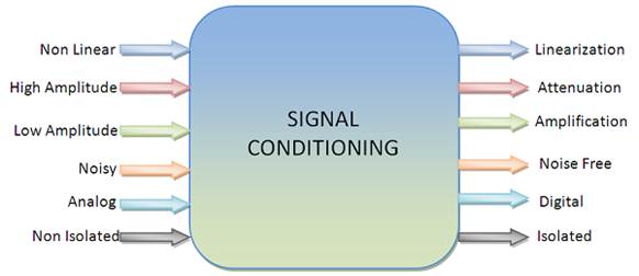
Fig. 5.1.1. Signal
conditioning operations
Amplification/Attenuation
Various applications of
Mechatronics system such as machine tool control unit of a CNC machine tool
accept voltage amplitudes in range of 0 to 10 Volts. However many sensors
produce signals of the order of milli volts. This low level input signals from
sensors must be amplified to use them for further control action. Operational
amplifiers (op-amp) are widely used for amplification of input signals. The
details are as follows.
Operational
amplifier (op-amp)
Operational Amplifier is a
basic and an important part of a signal conditioning system. It is often
abbreviated as op-amp. Op-amp is a high gain voltage amplifier with a
differential input. The gain is of the order of 100000 or more. Differential
input is a method of transmitting information with two different electronic
signals which are generally complementary to each other. Figure 2.6.2 shows the
block diagram of an op-amp. It has five terminals. Two voltages are applied at
two input terminals. The output terminal provides the amplified value of
difference between two input voltages. Op-amp works by using the external power
supplied at Vs + and Vs – terminals.
In general op-amp amplifies
the difference between input voltages (V+ and V-). The output of an operational
amplifier can be written as:
Vout = G * (V+ – V) (5.1)
where
G is Op-amp Gain.
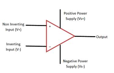
Fig. 5.1.2. Circuit diagram of an Op-amp
5.2. BAND PASS
FILTER
In some applications, we
need to filter a particular band of frequencies from a wider range of mixed
signals. For this purpose, the properties of low-pass and high-pass filters
circuits can be combined to design a filter which is called as band pass filter.Band
pass filter can be developed by connecting a low-pass and a high-pass filter in
series as shown in figure 5.2.1.
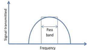
Fig. 5.2.1. Band pass filter
These filters pass all
frequencies above and below a particular range set by the
operator/manufacturer. They are also known as band stop filters or notch
filters. They are constructed by connecting a low-pass and a high-pass filter
in parallel as shown in Figure 5.2.2.
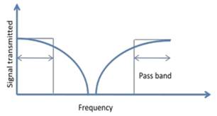
Fig. 5.2.2. Band reject
filter
5.3. PROTECTION,
CONVERSION AND PULSE WIDTH MODULATION
Protection
In many situations sensors
or transducers provide very high output signals such as high current or high
voltage which may damage the next element of the control system such as
microprocessor.
Protection from
high current
The high current to flow in
a sensitive control system can be limited by:
1. Using a series of
resistors;
2. Using fuse to break the
circuit if current value exceeds a preset or safe value.
Protection from
high voltage
Zener diode circuits are
widely used to protect a mechatronics control system from high values of
voltages and wrong polarity. Figure 5.3.1 shows a typical Zener diode circuit.
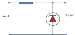
Fig. 5.3.1. Zener diode
circuit diagram
Zener diode acts as ordinary
or regular diodes upto certain breakdown voltage level when they are
conducting. When the voltage rises to the breakdown voltage level, Zener diode
breaks down and stops the voltage to pass to the next circuit. Zener diode as
being a diode has low resistance for current to flow in one direction through
it and high resistance for the opposite direction. When connected in correct
polarity, a high resistance produces high voltage drop. If the polarity reverses,
the diode will have less resistance and therefore results in less voltage drop.
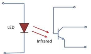
Fig. 5.3.2. Schematic of an
Optoisolator
In many high voltage
scenarios, it is required to isolate the control circuit completely from the
input high voltages to avoid the possible damage. This can be achieved by Optoisolators.
Figure 5.3.2 shows the typical circuit of an Optoisolator. It comprises of a
Light emitting diode (LED) and a photo transistor. LED irradiates infra red due
to the voltage supplied to it from a microprocessor circuit. The transistor
detects irradiation and produces a current in proportion to the voltage
applied. In case of high voltages, output current from Optoisolator is utilized
for disconnecting the power supply to the circuit and thus the circuit gets
protected.
Wheatstone
bridge
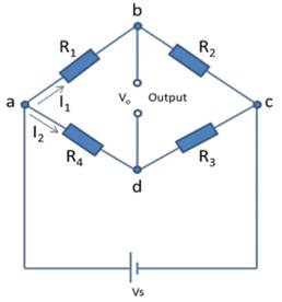
Fig. 5.3.3. Configuration of
a Wheatstone bridge
Wheatstone bridge is used to
convert a resistance change detected by a transducer to a voltage change.
Figure 5.3.3 shows the basic configuration of a Wheatstone bridge.
Pulse modulation
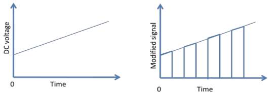
Fig. 5.3.4. Pulse amplitude
modulation

Fig. 5.3.5. Pulse width
modulation
During amplification of low
level DC signals from a sensor by using Op-amp, the output gets drifted due to
drift in the gain of Op-amp. This problem is solved by converting the analogue
DC signal into a sequence of pulses. This can be achieved by chopping the DC
signal in to a chain of pulses as shown in Figure 5.3.4. The heights of pulses
are related to the DC level of the input signal. This process is called as
Pulse Width Modulation (PWM). It is widely used in control systems as a mean of
controlling the average value of the DC voltage. If the width of pulses is
changed then the average value of the voltage can be changed as shown in Figure
5.3.5. A term Duty Cycle is used to define the fraction of each cycle for which
the voltage is high. Duty cycle of 50% means that for half of the each cycle,
the output is high.
5.4. DATA
CONVERSION DEVICES
Data Conversion Devices are
very important components of a Machine Control Unit (MCU). MCUs are controlled
by various computers or microcontrollers which are accepting signals only in
Digital Form i.e. in the form of 0s
and 1s, while the signalsreceived
from signal conditioning module or sensors are generally in analogue form
(continuous). Therefore a system is essentially required to convert analog
signals into digital form and vis-à-vis. Analog to Digital Converter is
abbreviated as ADC. Figure 5.4.1 shows a typical control system with data
conversion devices.
Based on the signals received
from sensors, MCU generates actuating signals in the Digital form. Most of the
actuators e.g. DC servo motors only accept analogue signals. Therefore the
digital signals must be converted into Analog form so that the required
actuator can be operated accordingly. For this purpose Digital to Analog
Converters are used, which are abbreviated as DACs. In subsequent sections we
will be discussing about various types of ADC and DAC devices, their principle
of working and circuitry.
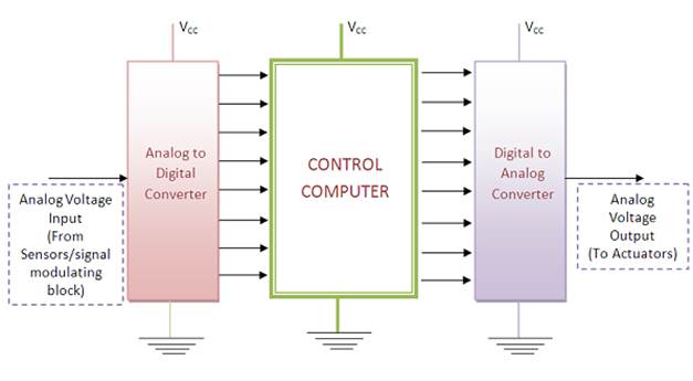
Fig. 5.4.1. A control system
with ADC and DAC devices
Comparators
In general ADCs and DACs
comprise of Comparators. Comparator is a combination of diodes and Operational
Amplifiers. A comparator is a device which compares the voltage input or
current input at its two terminals and gives output in form of digital signal
i.e. in form of 0s and 1s indicating which voltage is higher.
If V+ and V– be input voltages at two terminals of comparator then output of
comparator will be as:
V+ > V– ![]() Output 1;
Output 1;
V+ < V– ![]() Output 0.
Output 0.
Encoders
Though the output obtained
from comparators are in the form of 0s
and 1s, but can’t be called as binary
output. A sequence of 0s and 1s will
be converted into binary form by using a circuit called Encoder. A simple
encoder converts 2n input
lines into «n» output lines. These «n» output lines follow binary algebra.
Analog to
Digital Converter (ADC)
As discussed in previous
section ADCs are used to convert analog signals into Digital Signals. There are
various techniques of converting Analog Signals into Digital signals which are
enlisted as follows. However we will be discussing only Direct Conversion ADC, detail study of other
techniques is out of the scope of the present course:
a.
direct
conversion ADC or flash ADC;
b.
successive
approximation ADC;
c.
a ramp-compare ADC;
d.
wilkinson ADC;
e.
integrating ADC;
f.
delta-encoded ADC
or counter-ramp;
g.
pipeline ADC (also
called subranging quantizer);
h.
sigma-delta ADC
(also known as a delta-sigma ADC);
i.
time –
interleaved ADC.
Direct
Conversion ADC or Flash ADC
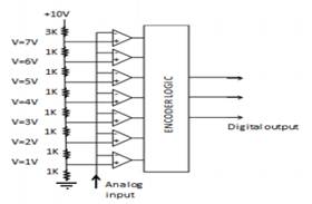
Fig. 5.4.2. Circuit of Flash
ADC
Figure 5.4.2 shows the
circuit of Direct conversion or Flash ADC. To convert a digital signal of
N-bits, Flash ADC requires 2N - 1 comparators and 2N
resistors. The circuit provides the reference voltage to all the comparators.
Each comparator gives an output of 1 when its analog voltage is higher than
reference voltage or otherwise the output is 0. In the above circuit, reference
voltages to comparators are provided by means of resistor ladder logic.
The circuit described in
figure 5.4.2 acts as 3 Bit ADC device. Let us assume this ADC works between the
range of 0 – 10 Volts. The circuit requires 7 comparators and 8 resisters. Now
the voltages across each resistor are divided in such a way that a ladder of 1
volt is built with the help of 1K-Ohm resistances. Therefore the reference
voltages across all the comparators are 1 – 7 volts.
Now let us assume that an
input voltage signal of 2.5 V is to be converted into its related digital form.
As 2.5V is greater than 1V and 2V, first two comparators will give output as 1,
1. But 2.5V is less than 3, 4, 5, 6, 7 V values therefore all other comparators
will give 0s. Thus we will have
output from comparators as 0000011 (from top). This will be fed to the encoder
logic circuit. This circuit will first change the output in single high line
format and then converts it into 3 output lines format by using binary algebra.
Then this digital output from ADC may be used for manipulation or actuation by
the microcontrollers or computers.

